
ビア・テンティング、フィリング、およびビア・イン・パッド:依頼すべき事項
Distinguish a covered via from a filled and capped via, and prepare the right fabrication questions for exposed pads and dense PCB layouts.
ガイドを読む設計ファイルから完成部品まで
ファイルの準備、選択肢の理解、そして次の製作計画を始めましょう。プリント基板、アセンブリ、機械製造に関する明確なガイダンスを提供します。.
ガイドライブラリー
49 ガイド
Page 5 of 6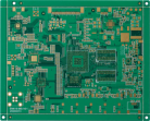
Distinguish a covered via from a filled and capped via, and prepare the right fabrication questions for exposed pads and dense PCB layouts.
ガイドを読む →
レイアウトを選択する前に、基板形状、部品間のクリアランス、部品間隔の必要性、および組み立て時の取り扱いやすさを考慮して、Vカット基板とタブ配線基板を比較してください。.
ガイドを読む →
製造上の問題を回避するため、完成寸法、めっきに関する注記、および位置合わせされた機械加工ファイルを含む、明確なPCBスロットおよびカットアウトデータを準備してください。.
ガイドを読む →
Understand plated and non-plated PCB holes, document finished sizes, and prevent mounting or connector holes from being misinterpreted.
ガイドを読む →
GerberプレビューでPCBサイズの誤りを診断します。注文前に、単位、余剰外形形状、パネル寸法、最終エクスポートを確認してください。.
ガイドを読む →
明確なリリースパッケージと変更履歴を使用して、見積書、アセンブリファイル、テスト結果を同じ基板リビジョンに紐づけてください。.
ガイドを読む →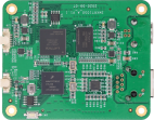
Check part identity, pin numbers, land patterns and mechanical access before committing a board to fabrication.
ガイドを読む →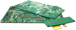
経験則だけで銅の重量を選ぶのではなく、実用的な電流経路仕様を作成する。.
ガイドを読む →
Compare the practical questions behind surface-finish selection, from pad flatness to contact requirements and purchasing notes.
ガイドを読む →準備ができたら
サービスを選択し、ファイルを共有して、プロジェクトの要件を確認してください。.