
Via Tenting, Filling and Via-in-Pad: What to Request
Distinguish a covered via from a filled and capped via, and prepare the right fabrication questions for exposed pads and dense PCB layouts.
Read guideFROM DESIGN FILES TO FINISHED PARTS
Prepare your files, understand your options and plan your next build. Clear guidance for PCBs, assembly and mechanical manufacturing.
THE GUIDE LIBRARY
49 guides
Page 5 of 6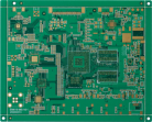
Distinguish a covered via from a filled and capped via, and prepare the right fabrication questions for exposed pads and dense PCB layouts.
Read guide →
Compare V-cut and tab-routed PCB panels by board shape, component clearance, separation needs and assembly handling before choosing a layout.
Read guide →
Prepare clear PCB slot and cutout data with finished dimensions, plating notes and aligned mechanical files to avoid fabrication questions.
Read guide →
Understand plated and non-plated PCB holes, document finished sizes, and prevent mounting or connector holes from being misinterpreted.
Read guide →
Diagnose an incorrect PCB size in a Gerber preview. Check units, stray outline geometry, panel dimensions and the final export before ordering.
Read guide →
Use clear release packages and change notes to keep quotations, assembly files and test results tied to the same board revision.
Read guide →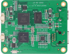
Check part identity, pin numbers, land patterns and mechanical access before committing a board to fabrication.
Read guide →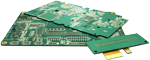
Build a useful current-path specification instead of choosing copper weight from a single rule of thumb.
Read guide →
Compare the practical questions behind surface-finish selection, from pad flatness to contact requirements and purchasing notes.
Read guide →WHEN YOU ARE READY
Choose a service, share your files and confirm the requirements for your project.