
PCB Silkscreen Checks: Keep Labels Useful After Assembly
Review PCB silkscreen for readable polarity, connector labels and revision marks without placing essential text on pads or under components.
Read guideFROM DESIGN FILES TO FINISHED PARTS
Prepare your files, understand your options and plan your next build. Clear guidance for PCBs, assembly and mechanical manufacturing.
THE GUIDE LIBRARY
41 guides matching “checklist”
Page 3 of 5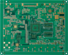
Review PCB silkscreen for readable polarity, connector labels and revision marks without placing essential text on pads or under components.
Read guide →
Write a PCBA functional test specification with power conditions, firmware, measurable pass limits and a clear failure-recording process.
Read guide →
Plan accessible PCB test points for power, programming and diagnostics, with a clear probe-side and fixture review before assembly.
Read guide →
Prevent stencil mismatches by checking board versus panel data, assembly side, frame requirements and the approved panel revision.
Read guide →
Plan PCB and panel fiducials with the assembler, including visibility, component clearance and consistent board and stencil revisions.
Read guide →
Review PCB placement coordinates and component orientation using a common origin, explicit board sides and an assembly drawing before release.
Read guide →
Document do-not-populate parts and assembly variants so the BOM, placement data and drawings describe the same finished board.
Read guide →
Create a clear BOM substitution process that checks the exact part, package and design requirements before an alternative enters assembly.
Read guide →
Prepare a controlled-impedance PCB request with target values, layer references, geometry and a clear approval process for stackup changes.
Read guide →WHEN YOU ARE READY
Choose a service, share your files and confirm the requirements for your project.